Phil's Patent Picks
Every now and again we hear of a new product or technology that is set to change the way we work or interact with the world around us. These innovative ideas are usually protected by patents particularly if there is potential for the invention to be copied or used in multiple applications.
The Printed Electronics sector is a a rich source of new ideas and industry developments. As time permits, I hope to bring you analysis of some of the patents and patent applications that are emerging. These patent picks are being featured on my blog and I encourage you to visit that site and subscribe. In that way you will be alerted to new items and will have access to all the previous posts.
The most recent posts are shown below:
Printed Electronics adds security to your Banknotes
Posted on 15 July 2016 by Phil C
Sipca, a company founded in 1927, provides secured identification, traceability and authentication solutions and services. A core component of their security expertise is the use of security inks that protect the majority of the worlds banknotes. I was interested to notice that earlier this year they filed a patent application combining the use of security inks with flexible printed electronics features to further enhance the security aspects of banknotes.
The patent application is WO2016037895, published on 17 March 2016, the inventors being Brahim Kerkar and Philippe Amon.
Most recent(amended) claim 1 is:
A banknote comprising: one or more security features, at least two flexible printed electronic (FPE) elements embedded in the banknote, at least one of the one or more security features and at least one of the at least two FPE elements have an interrelationship with each other, and a plurality of the at least two FPE elements have an interrelationship with each other, characterized in that each FPE element contains one or more security features comprising a chemical key represented with a set of molecules having different absorption or emission spectra, preferably said banknote comprising n FPE elements and m luminescent compounds, providing n*m potential combinations of secure FPEs dispatched in each banknote.
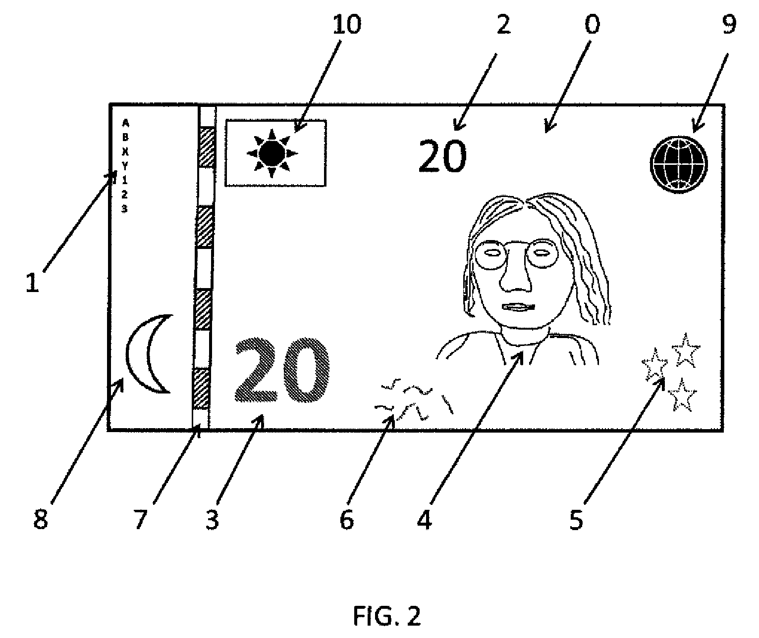
A typical banknote is shown in Fig 2 above (taken from the patent application) and has a variety of features for added security such as a substrate (0), a flag (10) and security features being a serial number (1 ), value numbers (2; 3) (wherein one of said value number is made of a colorshifting ink), an intaglio printed design (4), patterns made of a luminescent ink (5), luminescent fibers (6) incorporated in the substrate (0); a security thread (7), a transparent window (8) and a hologram (9).
The invention describes a banknote which has at least 2 FPE elements and these are designed to relate to each other and to the other security elements to provide the authentication mechanism. Various modes of operation are described including the ability for the FPE to be capable of additional features such as being configured to interact, for example, with a computer and/or a mobile phone.
One example provided is if a banknote having added FPE features is stolen, the owner, for example, using a mobile phone already containing the data related to the banknote (e.g., in a storage device) can send a communication to (e.g., all banks around the world), identifying the banknote as stolen, to be sure that the banknote is identified as stolen and/or is no longer valid. In other embodiments, the FPE may be operable to send a signal to the owners mobile device when a banknote belonging to the owner is used. Thus, if the banknote is stolen, when the thief attempts to use the stolen banknote, the owner is notified, and can contact the police. The embedded FPE may also provide traceability capabilities for the banknote, so that, for example, a location of the stolen banknote can be determined.
Phils Comments:
This is a further example of the way flexible printed electronics can enhance the practical usefulness of everyday things. The examples here also include security aspects which in itself is a huge technology field for the detection of counterfeiting and theft. The secret is the ability to make these FPE elements small enough and self contained to work over a long period without the need for a separate power source. Passive RFID elements are now very common and in everyday use.
3D Printed Electronics the next disruptive technology?
Posted on March 13, 2015 by Phil C
A patent application published on the last day of 2014 could easily have gone unnoticed but I believe it could be one of the next major breakthroughs in printed electronics. The application has the title PRINTED THREE-DIMENSIONAL (3D) FUNCTIONAL PART AND METHOD OF MAKING and can be viewed by clicking on the link: WO2014209994. The technology has been developed in the Research labs of Professor Jennifer Lewis at Harvard University. The Lewis Lab team have been working for some years on multiple technologies including 3d printing, conductive inks for printed electronics, composite materials and micro-batteries. This patent application describes various embodiments of a 3D functional part, for example one of the paragraphs states:
A method of printing a 3D functional part comprises, according to another embodiment: forming one or more portions of a 3D structure using a 3D printing method; positioning at least one functional electronic device on an exposed surface of the one or more portions; and forming conductive interconnects to and from the at least one functional electronic device using a 3D printing method. The method may further comprise, in some embodiments, forming one or more additional portions of the 3D structure using a 3D printing method. The one or more additional portions of the 3D structure may at least partially cover the at least one functional electronic device.
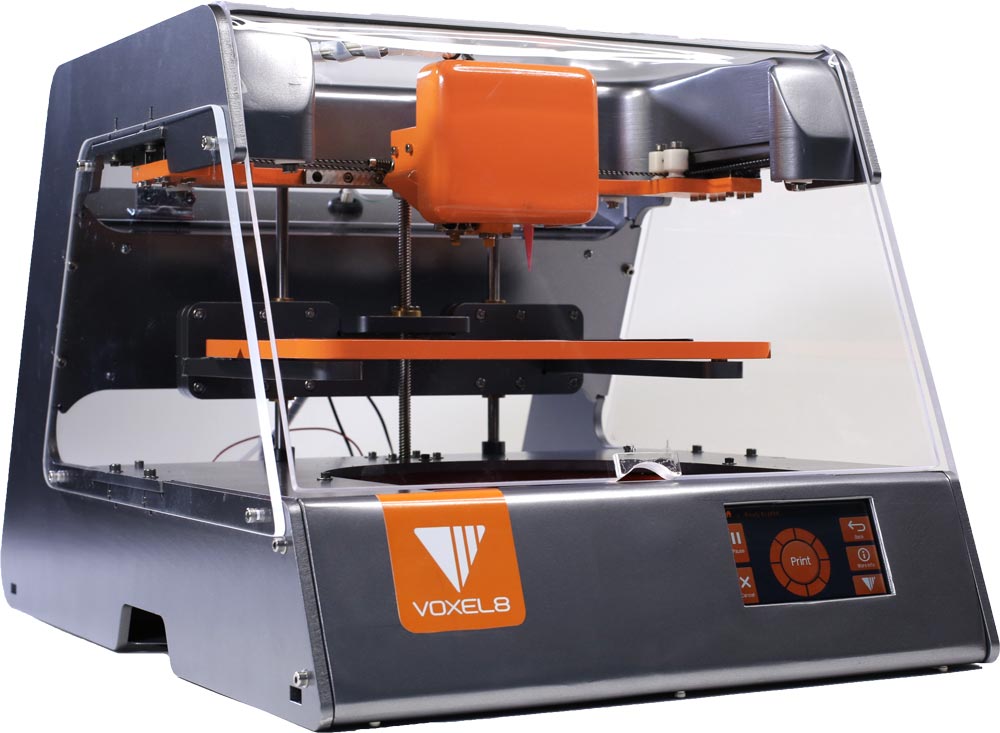
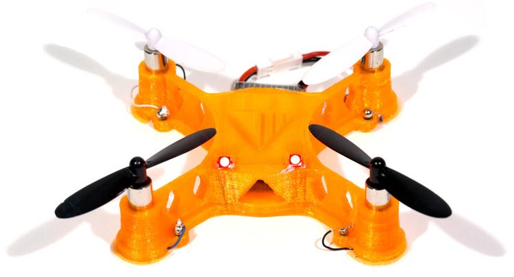
The method uses a printer with at least 2 printheads so that you can co-print both a matrix material and a conductor. Electronic components can be manually inserted while the 3D printing operation is temporarily halted and then overprinted to embed the device. One of the advantages of a direct write printing action that can move in all three axes is that the functional electronic devices can be orientated at any angle in the 3d structure and the conductive filaments are not constrained to a planar pathway as is typical of PCB boards. The reader can refer to the patent application for more details of the materials for the matrix and the conductive inks but better still I refer you to the spin out company Voxel8 that plans to release this 3D printed electronics platform towards the end of 2015. The patent application has a priority date of 24 June 2013. This is an impressive time from filing the technology to a commercial device. The first announcement of the 3D printer was made at CES 2015 back in early January.
Their promotional website can be found here. I have included an image of the printer along with one of the devices made on it.
Phils comments:
3D printing continues to be an exciting area with many opportunities for prototyping and with the improvement in print heads and materials the devices are becoming more robust to the point that 3D printed components are now as good as their traditionally made counterparts. The technology described here allows embedded electronics to be included in the 3D printing process. Voxel8 will leverage ink designs from the Lewis research group, including those that enable 3D printing of resistors, dielectrics, stretchable electronics and sensors, and even lithium ion batteries. I expect to see a significant number of patent applications emerge as part of this patent family and then further new applications as the materials and processes are developed.
I would like to thank Arthur Berman who contacting me for an opinion on this technology which then prompted me to write the article.
Printed Electronics card with piezo-powered indicator
Posted on March 3, 2015 by Phil C
I came across a recently granted patent that describes a printed
card such as a business card with a display that is powered by a
built-in piezo power source. This is a neat printed electronics
application that gets around the problem of needing a battery to
operate any device such as an indicator or display printed on the
substrate. Although there are printed electronics batteries they
tend to require encapsulated electrolytes to fabricate them and so
are not entirely compatible with low-cost printing processes.
The patent is US8959734
and was published on 24th Feb 2015. It has a priority date of 16th
Dec 2010. Details of the inventors and assignee are summarised below
along with the abstract:
Inventors: Daniel; Jurgen H. (San Francisco, CA), Ng; Tse Nga
(Mountain View, CA)
Assignee: Palo Alto Research Center Incorporated (Palo Alto, CA)
Abstract
An interactive card or the like employs a piezoelectric charge
generator (piezo-strip) for temporarily driving an indicator. The
piezo-strip may be displaced (bent) in order to generate charge to
drive the indicator. Printed electronic processes are utilized to
produce the indicator and/or the piezoelectric charge generator. An
indicator is formed on a substrate by way of a printed electronics
process. A displaceable region of piezoelectric material associated
with the said substrate is formed by way of a printed electronics
process. Electrical interconnections are formed on said substrate by
way of a printed electronics process. The electrical
interconnections connecting said indicator and said first region of
piezoelectric material such that displacement of said first region
of piezoelectric material generates a voltage therein that is
provided to said indicator in order to actuate said indicator and
thereby indicate the displacement of said first region of
piezoelectric material.
The drawings give a pretty good idea of the invention and its
construction. Ive reproduced two sets of figures below to show this
but there are more in the patent that you can view.


FIG. 1 is an illustration of a display-capable business card with
piezo-strip according to an embodiment of the present disclosure.
FIG. 2 is an illustration of the display-capable business card with
piezo-strip according to FIG. 1, showing the deflection of the
piezo-strip and the resulting actuation of an indicator.
FIG. 5 is a photograph of a display-capable business card with
piezo-strip and template over an indicator according to another
embodiment of the present disclosure.
FIG. 6 is a photograph of the components of the display-capable
business card with piezo-strip and template over an indicator shown
in FIG. 5.
Claim 1 provides the legal statement that defines the invention:
1. A method of forming an interactive card with indicator on a
substrate, comprising: forming said indicator on said substrate by
way of a printed electronics process; forming a displaceable region
of piezoelectric material associated with said substrate by way of a
printed electronics process; forming electrical interconnections on
said substrate connecting said indicator and said first region of
piezoelectric material such that displacement of said first region
of piezoelectric material generates a voltage therein that is
provided to said indicator in order to actuate said indicator and
thereby indicate the displacement of said first region of
piezoelectric material, said electrical interconnections formed by
way of a printed electronics process, wherein said first region of
piezoelectric material is formed over a piezo-strip region of said
substrate; and partially disconnecting said piezo-strip region from
said substrate in order to permit displacement of said piezo-strip
region independently from the remainder of said substrate.
Phils comments:
Piezo technology does offer quite a few opportunities for where a brief amount of power is required to trigger a device. This patent describes one use illustrated above but also extends the ideas to other applications such as switches or sensors that can indicate if vibration or bending has happened. Another application detects liquid levels by sensing where the liquid moves a series of vertical flaps on the sensor by its swirling action. I have not seen any commercial applications of this but am aware of a Swiss company that uses the piezo effect to produce a keyboard and they recently demonstrated this integrated with one of Plastic Logics electrophoretic displays (see here).
Aqueous Conductive Silver Ink
Posted by Phil C on May 16, 2014Printed electronics is continuing to grow as more and more
applications are developed and commercialised. One of the key
stumbling blocks continues to be the practicalities of printing
narrow conductive tracks and the ease of use of the materials and
processes involved. One of the key system components, often
taken for granted, is the ink. The majority of
conductive ink compositions in use today are solvent-based thick
film systems designed for low speed screen printing. Water
based conductive inks and coatings offer significant ecological
advantages over solvent-based compositions, as the latter release
solvents into the atmosphere on drying. Aqueous conductive
inks, however, have so far not offered the high conductivity, or low
electrical resistivity, achievable with solvent-based formulas.
Sun Chemical Corp. have just been granted a patent for an aqueous
ink with high conductivity and good printing properties. This
invention more specifically relates to an aqueous conductive silver
ink suitable for use in RFID and other electronic technologies. The
composition is highly conductive and requires reduced drying energy.
In addition, it may be applied to low cost substrates via high speed
printing processes. The key components of the ink formulation
include: (meth)acrylic copolymer or salt thereof; conductive
particles; an anionic surface wetting agent; defoamer and
water. The first claim suggests the ink can be up to 80% water
depending on the amount of the other ingredients.
The patent is US8709288 and it was issued on 29 April
2014. The Inventors are Jason Rouse and Dave Klein.
The independent claims from the patent are listed below:
1. A method of forming a conductive
pattern on a substrate comprising applying a conductive composition
comprising (a) metallic silver conductive particles, (b) water
soluble styrene/(meth)acrylic copolymer, (c) an anionic wetting
agent, (d) defoamer and (e) 10 to 80% water, the composition
providing a sheet resistance of less than 0.83 ohms/sq, on the
substrate and drying the composition.
34. A method of forming a conductive pattern on a substrate
comprising applying a conductive composition consisting essentially
of (a) metallic silver conductive particles, (b) water soluble
styrene/(meth)acrylic copolymer, (c) an anionic surfactant, (d)
defoamer and (e) 10 to 80% water, the composition providing a sheet
resistance of less than 0.83 ohms/sq, on the substrate and drying
the composition.
37. A method of forming a conductive pattern on a substrate
comprising applying a conductive composition consisting of (a)
metallic conductive particles, (b) water soluble
styrene/(meth)acrylic copolymer, (c) an anionic surfactant, (d)
defoamer, (e) 10 to 80% water, and optionally another solvent, the
composition providing a sheet resistance of less than 0.83 ohms/sq,
on the substrate and drying the composition.
The differences above are subtle but important, claim 34 describes
the composition with an anionic surfactant rather than a wetting
agent, and claim 37 describes a more general formulation with any
metallic conductive particle and optionally includes another
solvent. Each claim includes the requirement that the
composition provides a resistance of less that 0.83 ohms/sq on the
substrate.
Phils Comments:
Good to see that research into inks suitable for printed
electronics is providing environmentally acceptable
formulations. Reducing solvents and also reducing the energy
requirements for drying are all good directions for the ink
design. We sometimes forget the huge demand put upon the inks
we use, for example they need good abrasion and chemical resistance
when dried so that they are not easily scratched or wiped off during
subsequent uses, they need to have proper rheology and substrate
wetting properties to obtain good ink transfer and graphic
reproduction. Additionally, the ink should possess good flexibility
and thermal stability to withstand the physical deformation to which
the substrate may be subjected. Lets remember the research
that goes into the inks when we next see a printed electronics
design in use!
Thinking Ink allows printed packaging to interact with smartphones
Posted by Phil C on February 24, 2014A recent patent lawsuit filed by Touchpac Holdings against TouchBase Technologies Inc. has highlighted the US Patent US8497850 which is owned by Printechnologics GmbH (T+Ink). Details of the lawsuit were reported by Printed Electronics World in their article on 18 Feb 2014.
The patent was granted on 30 July 2013 and describes the technology that T+Ink have developed and called Touchcode. This is a highly secure printed conductive ink signature embedded in packaging, labels and other objects that a smartphone or other sensing device can detect through capacitive touch. The patent provides some detail of the system which is defined in independent claim 22:
A system comprising: a. an information
carrier comprising a dielectric and/or conductive pattern which
encodes information, and wherein the information carrier (1)
comprises a substrate (2) with a first dielectric coefficient ∈1 and
a second material with a second dielectric coefficient ∈2, the
second coefficient ∈2 being different from the first coefficient ∈1,
or wherein the information carrier (1) comprises a substrate (2)
with a first conductivity σ1 and a second material with a second
conductivity σ2, the second conductivity σ2 being different from the
first conductivity σ1, b. a detection device having a capacitive
touch screen; the detection device decodes the information upon
interaction between the information carrier and the touch screen,
wherein the interaction is based on a difference in the dielectric
coefficient and/or the conductivity of the pattern, wherein the
interaction is induced by relative motion between the information
carrier and the touch screen.
A more visual explanation can be found on the T+Ink Touchcode website. As explained on the website, Touchcode is an invisible electronic code printed on paper, cardboard, film or labels. Just put the product on the display of your smartphone/tablet/multitouch device to read the data. In this way you can add interactivity to just about any product. The system is similar to QR codes, barcodes or other tags but does not require activating a camera app on the phone or tablet to work.